- 您现在的位置:买卖IC网 > Sheet目录473 > MAX2656EVKIT (Maxim Integrated)EVAL KIT
�� �
�
�1575MHz/1900MHz� Variable-IP3�
�Low-Noise� Amplifiers�
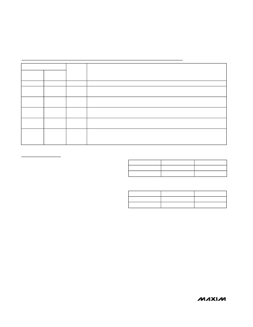
�Pin� Description�
�PIN�
�MAX2654�
�1�
�2,� 5�
�–––�
�3�
�4�
�MAX2655/�
�MAX2656�
�–––�
�2,� 5�
�1�
�3�
�4�
�NAME�
�GND�
�GND�
�BIAS�
�RFIN�
�V� CC�
�DESCRIPTION�
�Ground.� Connect� to� the� PC� board� ground� plane� through� a� 0.017in� x� 0.035in� line.�
�Ground.� Connect� to� the� PC� board� ground� plane� with� as� low� an� inductance� path� as�
�possible.�
�Bias� Control.� Connect� a� resistor� R� BIAS� from� BIAS� to� GND.� R� BIAS� sets� IP3� and�
�supply� current.�
�Amplifier� Input.� Requires� a� DC-blocking� capacitor� and� external� matching� components.�
�Supply� Voltage.� Bypass� to� ground� with� an� appropriate� capacitor� as� close� to� the� IC� as�
�possible.� Refer� to� MAX2654/MAX2655/MAX2656� EV� kits� for� capacitor� values.�
�RF� Output.� Incorporates� an� internal� DC-blocking� capacitor.� RFOUT� is� internally�
�6�
�6�
�RFOUT�
�matched� to� 50� ?� .� DC� bias� on� this� pin� selects� gain� mode� (MAX2656)� or� shutdown� mode�
�(MAX2654/MAX2655)� (see� Applications� Information� ).�
�Detailed� Description�
�Table� 1.� R� BIAS� vs.� IP3� for� MAX2655�
�The� MAX2654/MAX2655/MAX2656� are� low-noise� ampli-�
�fiers� designed� for� applications� in� GPS� receivers,� satel-�
�lite� and� PCS� phones.� The� MAX2655/MAX2656� feature�
�variable� IP3s,� adjusted� by� a� single� external� bias� resis-�
�R� BIAS� (� ?� )�
�698�
�357�
�IP3� (dBm)�
�2.2�
�3.8�
�I� CC� (mA)�
�5.8�
�10.1�
�tor.� Another� feature� of� the� MAX2654/MAX2655� is� a�
�power� shutdown� control� mode,� eliminating� the� need� for�
�an� external� supply� switch.� The� MAX2656� features� a�
�Table� 2.� R� BIAS� vs.� IP3� for� MAX2656�
�high-� and� low-gain� control� mode� selected� by� an� exter-�
�nal� logic� control.�
�Input� and� Output� Ports�
�R� BIAS� (� ?� )�
�715�
�511�
�IP3� (dBm)�
�-3�
�1.5�
�I� CC� (mA)�
�8.5�
�11.5�
�The� MAX2654/MAX2655/MAX2656� incorporate� on-chip�
�matching� networks� to� 50� ?� at� the� output� ports,� eliminat-�
�ing� the� need� for� external� matching� components.� (For�
�MAX2655,� a� shunt� inductor� is� recommended� for� best�
�output� return� loss.� Refer� to� the� MAX2655� EV� kit�
�schematic.)� The� MAX2654/MAX2655/MAX2656� require�
�simple� matching� networks� at� the� input� ports.� The� values�
�of� these� matching� components� are� recommended� in�
�the� Typical� Operating� Circuit.�
�Variable� IP3�
�The� IP3� of� MAX2655� and� MAX2656� is� adjusted� through�
�an� external� resistor� (R� BIAS� ).� Tables� 1� and� 2� summarize�
�the� values� of� R� BIAS� for� different� IP3s� for� MAX2655� and�
�MAX2656.�
�Gain-Step� Control� (MAX2656)�
�The� DC� bias� voltage� at� RFOUT� of� the� MAX2656� serves�
�as� a� gain-step� control� input.� When� the� applied� DC� volt-�
�age� at� RFOUT� through� a� 10k� ?� resistor� is� less� than�
�+0.6V,� the� device� is� in� high-gain� mode.� When� the�
�applied� DC� voltage� is� greater� than� +2.0V,� the� device�
�gain� is� attenuated� by� 13dB.� A� standard� logic� output�
�can� be� applied� as� shown� in� the� Typical� Operating�
�Circuit� .�
�Shutdown-Enable� (MAX2654/MAX2655)�
�The� DC� bias� voltage� at� RFOUT� of� the� MAX2654/�
�MAX2655� serves� as� a� shutdown� enable� input.� When� the�
�applied� DC� voltage� at� RFOUT� through� a� 10k� ?� resistor�
�is� less� than� +0.6V,� the� device� is� in� shutdown� mode.�
�When� the� DC� voltage� is� greater� than� +2V,� the� device� is�
�enabled.�
�12�
�______________________________________________________________________________________�
�发布紧急采购,3分钟左右您将得到回复。
相关PDF资料
MAX2658AEVKIT+
KIT EVALUATION FOR MAX2658
MAX2659EVKIT+
KIT EVAL FOR MAX2659 LNA
MAX2664EVKIT+
EVAL KIT MAX2664
MAX2666EVKIT+
EVAL KIT MAX2666
MAX2669EVKIT+
KIT EVALUATION FOR MAX2669
MAX2670GTB+TW
IC FRONT-END AMP GPS/GNSS 10TDFN
MAX2673EVKIT
EVAL KIT MAX2673
MAX2676EVKIT+
EVAL KIT MAX2676
相关代理商/技术参数
MAX2656EXT
制造商:Maxim Integrated Products 功能描述:6 PIN COUNT SC70 PACKAGE TYPE - Bulk 制造商:Rochester Electronics LLC 功能描述:
MAX2656EXT+
制造商:Maxim Integrated Products 功能描述:RF AMP CHIP SGL GP 2GHZ 5.5V 6PIN SC-70 - Rail/Tube
MAX2656EXT+T
功能描述:射频放大器 1575MHz/1900MHz Variable-IP3 RoHS:否 制造商:Skyworks Solutions, Inc. 类型:Low Noise Amplifier 工作频率:2.3 GHz to 2.8 GHz P1dB:18.5 dBm 输出截获点:37.5 dBm 功率增益类型:32 dB 噪声系数:0.85 dB 工作电源电压:5 V 电源电流:125 mA 测试频率:2.6 GHz 最大工作温度:+ 85 C 安装风格:SMD/SMT 封装 / 箱体:QFN-16 封装:Reel
MAX2656EXT-T
功能描述:射频放大器 1575MHz/1900MHz Variable-IP3 RoHS:否 制造商:Skyworks Solutions, Inc. 类型:Low Noise Amplifier 工作频率:2.3 GHz to 2.8 GHz P1dB:18.5 dBm 输出截获点:37.5 dBm 功率增益类型:32 dB 噪声系数:0.85 dB 工作电源电压:5 V 电源电流:125 mA 测试频率:2.6 GHz 最大工作温度:+ 85 C 安装风格:SMD/SMT 封装 / 箱体:QFN-16 封装:Reel
MAX2657AEVKIT+
功能描述:放大器 IC 开发工具
RoHS:否 制造商:International Rectifier 产品:Demonstration Boards 类型:Power Amplifiers 工具用于评估:IR4302 工作电源电压:13 V to 23 V
MAX2657EVKIT+
功能描述:放大器 IC 开发工具 MAX2657 Eval Kit
RoHS:否 制造商:International Rectifier 产品:Demonstration Boards 类型:Power Amplifiers 工具用于评估:IR4302 工作电源电压:13 V to 23 V
MAX2657EWT+
制造商:Maxim Integrated Products 功能描述:GPS/GNSS LOW-NOISE AMPLIFIERS - Rail/Tube
MAX2657EWT+T
功能描述:射频放大器 GPS/GNSS Low Noise Amp
RoHS:否 制造商:Skyworks Solutions, Inc. 类型:Low Noise Amplifier 工作频率:2.3 GHz to 2.8 GHz P1dB:18.5 dBm 输出截获点:37.5 dBm 功率增益类型:32 dB 噪声系数:0.85 dB 工作电源电压:5 V 电源电流:125 mA 测试频率:2.6 GHz 最大工作温度:+ 85 C 安装风格:SMD/SMT 封装 / 箱体:QFN-16 封装:Reel